
HIGH-SPEED PCB LAYOUT / 02
Type-C TBT + USB + DP 40G Retimer
Channel planning, via-stub control and reference-plane requirements around a retimer.
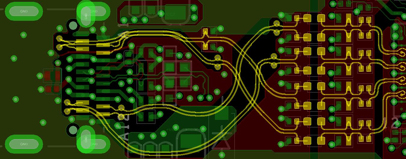
Topology notes
The following constraints are supplied for this design example. Apply them with the relevant platform design guide, retimer requirements and PCB stack-up.
CPU → Retimer
- Maximum allowed vias: 2 before the retimer.
- Maximum via stub length: 250 µm per via between the CPU and retimer.
Retimer → Post-channel
- Maximum allowed vias: 2 after the retimer.
- The retimer post-channel must have no via stub.
Routing style & RFI / EMI
- Microstrip (MS) main-route routing must be interleaved.
- Stripline (SL) is recommended instead of microstrip to reduce system RFI / EMI.
- If microstrip routing is necessary, follow the applicable EMC platform design guide (PDG) for RFI / EMI mitigation.
Reference-plane requirements
Microstrip
The reference plane must be continuous ground.
Stripline
Ground on both sides is strongly preferred. If necessary, one side may be a power plane with a low amount of low-frequency noise; the other side must be continuous ground.
Dual stripline
Ground on both sides is strongly preferred. If necessary, one side may be a power plane with a low amount of low-frequency noise. The other side must be continuous ground, and that ground plane must be closer to the signal route.
Layout focus
This example brings together differential-pair routing and the channel constraints on each side of the retimer. The layout image illustrates routing organization; via-stub lengths and reference-plane continuity require the PCB stack-up and design data to verify.
LET’S BUILD YOUR NEXT BOARD
Have a PCB project to discuss?
Send us your schematic, design requirements or existing PCB files.