
HIGH-SPEED PCB LAYOUT / 01
Zigzag Routing Layout Example
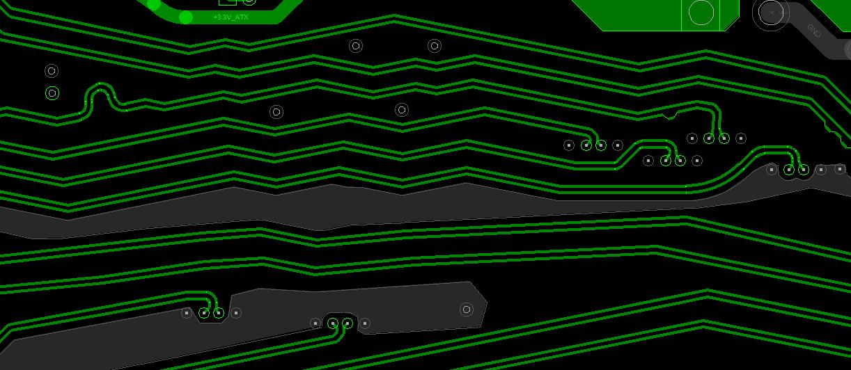
Angled differential-pair routing to address fiber-weave-related skew risk.
The routing challenge
Glass bundles and resin regions can expose the two traces of a differential pair to different dielectric conditions. Sustained alignment with the weave can contribute to propagation-delay mismatch.
Layout approach
The example shows repeated shallow-angle segments along paired traces. Segment direction and length are considered together with the laminate weave, available routing space and channel constraints.
Routing guidelines supplied for this example
- Use zigzag or angled routing with a minimum 10° angle relative to the fiber weave, where required by the applicable platform guide.
- Apply the method beyond the allowable RSS length specified by that guide; no numerical RSS limit was supplied for this example.
- Confirm the glass-fabric weave pitch with the board fabricator. The supplied guidance calls for segment lengths that cross two weave bundles.
- For the same forward distance, increasing the routing angle increases the trace length. Account for the additional length in the channel budget.
These are platform- and material-dependent guidelines, not universal dimensions for every PCB.
What this example demonstrates
Practical zigzag routing geometry and paired-trace organization. The image alone does not verify the routing angle against the actual weave, material pitch, skew reduction or electrical compliance. No simulation or measurement results are presented.
Technical reference
Intel’s public guidance discusses zigzag routing and a minimum 10° angle relative to the fiber weave. Refer to the applicable platform guide and actual laminate data for project-specific requirements.
Intel Agilex 7 High-Speed Serial Interface Signal Integrity Design Guidelines ↗
LET’S BUILD YOUR NEXT BOARD
Have a PCB project to discuss?
Send us your schematic, design requirements or existing PCB files.