
HIGH-SPEED PCB LAYOUT / 03
DDR5 UDIMM Tabbed Routing
Transfer Rate: 5600 MT/s
Local geometry compensation for impedance matching and far-end crosstalk control.
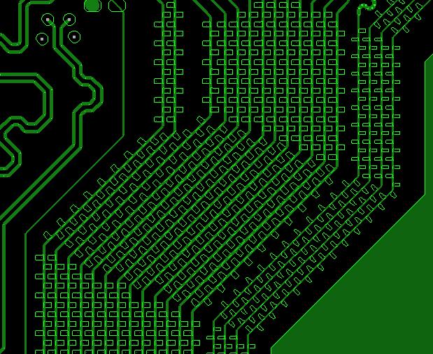
The routing challenge
Dense memory routing can constrain trace width and spacing. Narrow routing sections can introduce impedance discontinuities and reflections, while coupling between adjacent traces can increase far-end crosstalk (FEXT).
Tabbed routing approach
Small rectangular or trapezoidal tabs are added at selected intervals along the trace edges. Their dimensions and spacing provide a way to tune the local electrical behavior of the routing section.
Impedance compensation
Tabs add local conductor area and capacitive loading. Where narrow traces raise impedance, carefully sized tabs can lower the effective impedance toward the channel target, helping reduce reflections at routing transitions.
Far-end crosstalk control
Tabs can increase mutual capacitance between adjacent traces while affecting mutual inductance less strongly. Tuning the balance of capacitive and inductive coupling can reduce FEXT under the appropriate geometry and stack-up conditions.
Design considerations
Tab width, length, pitch and placement must be considered together with trace spacing, reference-plane distance and the PCB materials. The aim is to improve impedance consistency and coupling balance across the channel; the final geometry needs channel-specific simulation and verification.
Performance context
The supplied background cites a reduction in FEXT from 42 mV to 2 mV under specific conditions. This is a reference example, not a simulation or measurement result for the PCB shown here. The reference geometry, excitation and measurement conditions have not been supplied, so this numerical improvement is not claimed for this 5600 MT/s design.
LET’S BUILD YOUR NEXT BOARD
Have a PCB project to discuss?
Send us your schematic, design requirements or existing PCB files.