
HIGH-SPEED PCB LAYOUT / 05
Back Drilling
Removing unused via barrels to control stub resonance and preserve channel bandwidth.
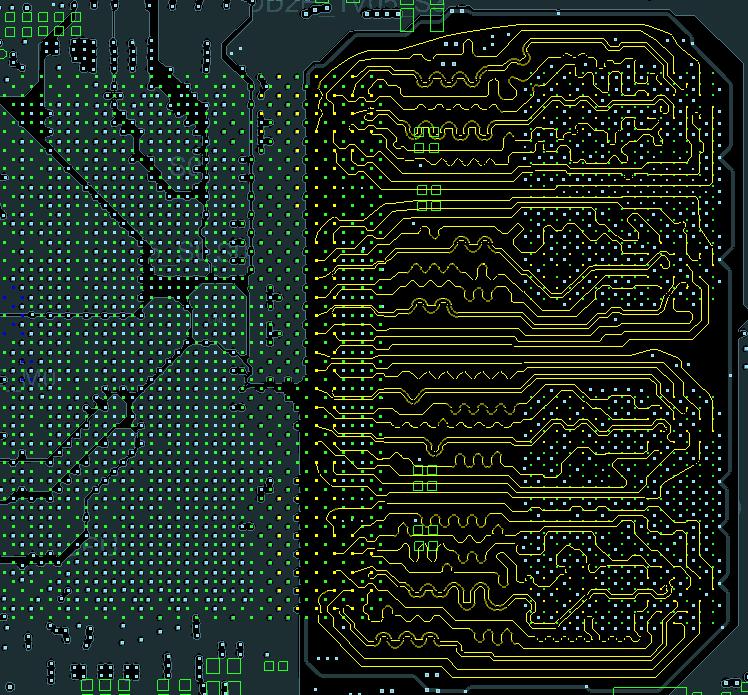
Why remove the via stub?
The unused plated barrel beyond a signal’s connected layer behaves as an open-ended transmission-line branch. Back drilling removes this excess copper to reduce reflections and resonance-related channel degradation.
Impedance discontinuity
The stub adds parasitic loading and changes the via transition’s impedance, causing reflections.
Resonance and transmission notches
Near a quarter wavelength in electrical length, an open-ended stub can present a low impedance at its junction with the signal path. Strong reflection can produce a deep transmission notch and increased insertion loss at that frequency. This is an electrical equivalent, not a physical short to ground.
Coupling and emissions
Unused via structures can contribute to unwanted coupling. The effects on crosstalk and EMI depend on via geometry, nearby signals and return-path design.
Eye opening and link margin
Reflections and resonance can reduce eye height and width and increase jitter, potentially degrading bit-error performance.
How back drilling works
After the through-hole is drilled and plated, a controlled-depth drilling operation uses a larger tool to remove the unused copper barrel from the appropriate board side while preserving the required layer connections. This example specifies drilling from the bottom side.
Shortening the residual stub moves its resonance to higher frequencies. Residual lengths around 8–10 mil (approximately 203–254 µm), or smaller where supported, are possible design targets rather than a universal process guarantee. The target must be agreed with the fabricator and checked against the channel bandwidth.
Back-drill fabrication legend
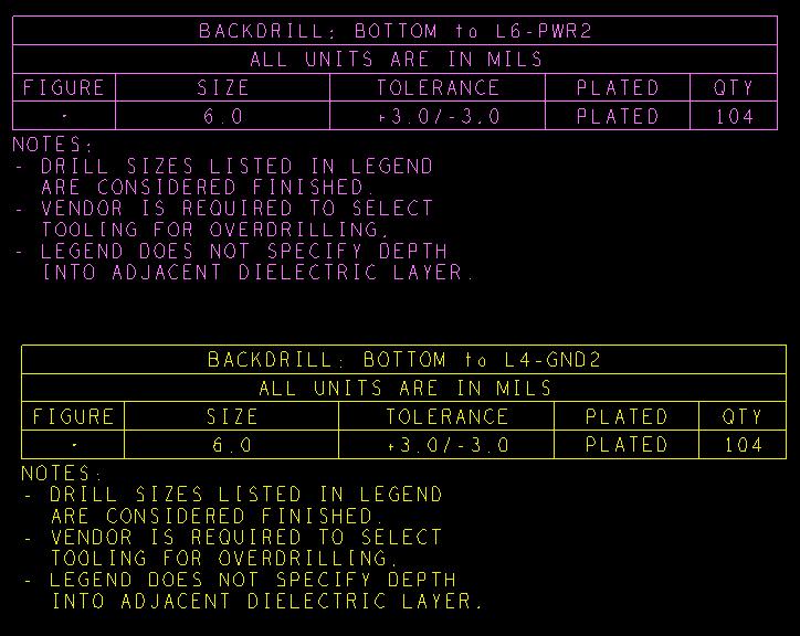
Each legend lists SIZE 6.0, TOLERANCE +3.0/−3.0, PLATED and QTY 104. The notes identify the listed sizes as finished sizes, require the vendor to select tooling for overdrilling, and state that the legend does not specify depth into the adjacent dielectric layer.
These legend entries should be read with the full fabrication drawing and stack-up. The SIZE entry is not a specified residual-stub length or a final back-drill tool selection. Confirm drilling depth, remaining stub, tool clearance and protection of the required connections with the fabricator.
Intended benefits
- Improve the via transition’s impedance response and reduce reflections.
- Reduce stub-related transmission notches and preserve usable channel bandwidth.
- Help improve eye opening and link margin.
- Reduce unwanted coupling where the stub is a contributing factor.
The supplied images document the layout and fabrication legend. The actual residual stub and electrical improvements require fabrication inspection and channel verification.
Technical reference: Intel AN 596 — via-stub resonance ↗
Technical reference: TI AFE79xx Layout Guide — back-drill stubs ↗
LET’S BUILD YOUR NEXT BOARD
Have a PCB project to discuss?
Send us your schematic, design requirements or existing PCB files.