
← All projects
SELECTED WORK / PCB LAYOUT
Xilinx SOM + Carrier Board
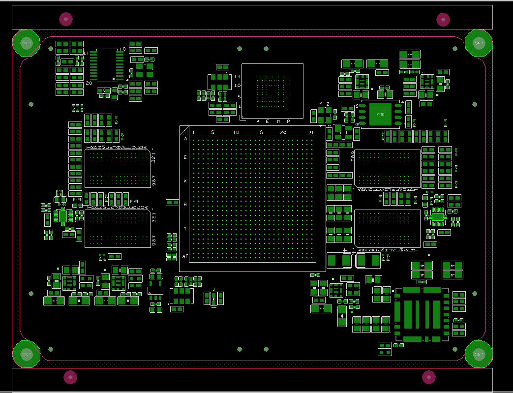
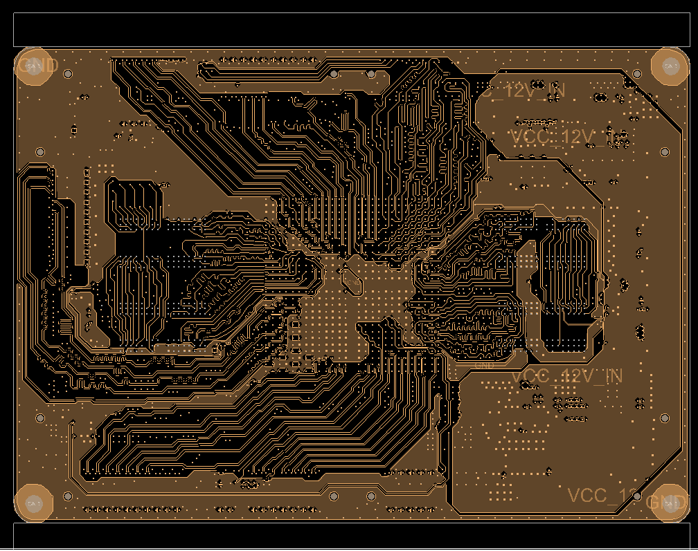
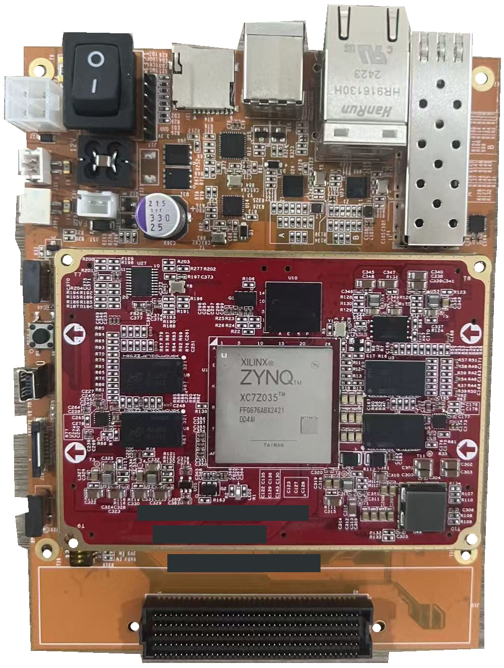
PCB layout for a Xilinx-based system-on-module and carrier-board project. The SOM combines a compact 102 × 72 mm outline with a 12-layer, through-hole PCB construction.



Use the arrows, thumbnails or swipe to browse. Select an image to view full size.
- Platform
- Xilinx-based FPGA
- SOM layer count
- 12 layers
- SOM dimensions
- 102 × 72 mm
- Design tool
- Cadence Allegro 16.6
- SOM via technology
- Through-hole vias
- Project interfaces
- LPDDR3 · PCIe Gen 2 · USB 3.2
PCB layout scope
SOM core-board and carrier-board PCB layout. Layer count and dimensions above refer specifically to the SOM; carrier-board specifications are not listed.
Project imagery
Original layout views show component placement and multilayer routing detail. The assembly photograph has its background removed and project identifiers redacted; SoC markings are retained.
LET’S BUILD YOUR NEXT BOARD
Have a PCB project to discuss?
Send us your schematic, design requirements or existing PCB files.