
← All projects
SELECTED WORK / PCB LAYOUT
MediaTek MT8321 3G Tablet Mainboard
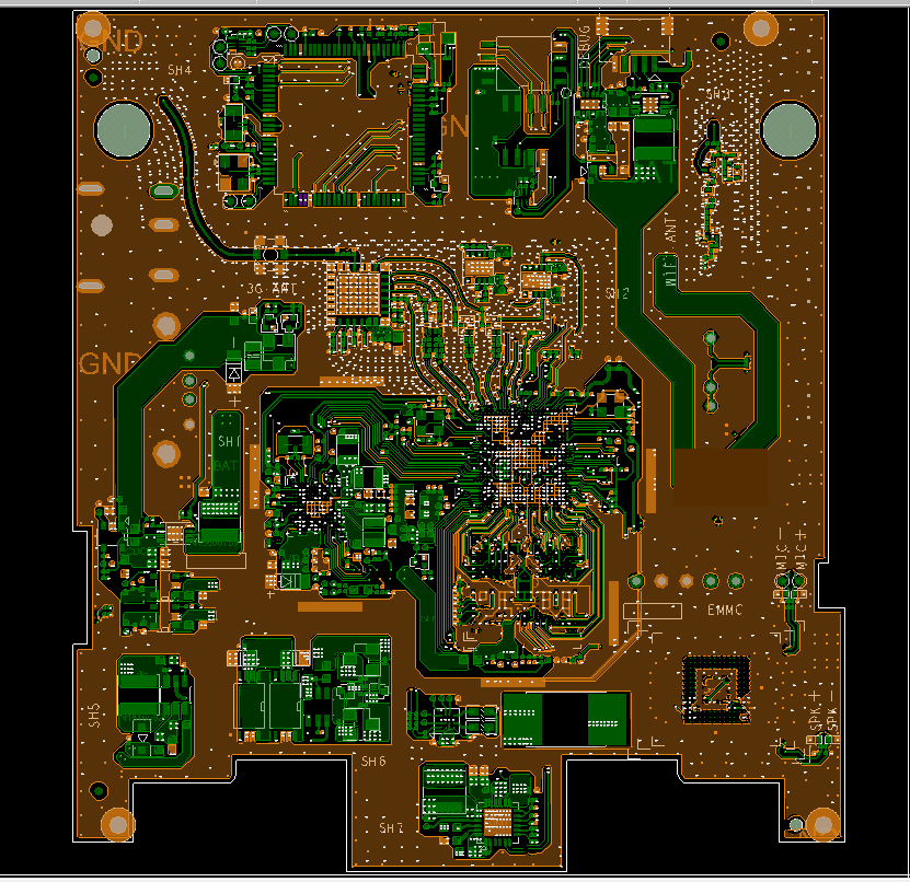
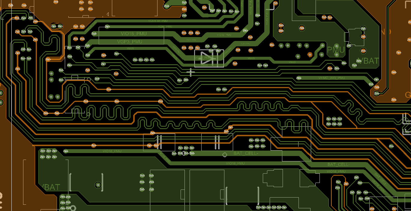
PCB layout for a MediaTek MT8321-based 3G tablet mainboard. The compact 6-layer, 85 × 78 mm design brings together processor, memory, power and RF routing.

Use the arrows, thumbnails or swipe to browse. Select an image to view full size.
- Platform
- MediaTek MT8321
- Layer count
- 6 layers
- Board dimensions
- 85 × 78 mm
- Design tool
- Cadence Allegro 17.2
- Via technology
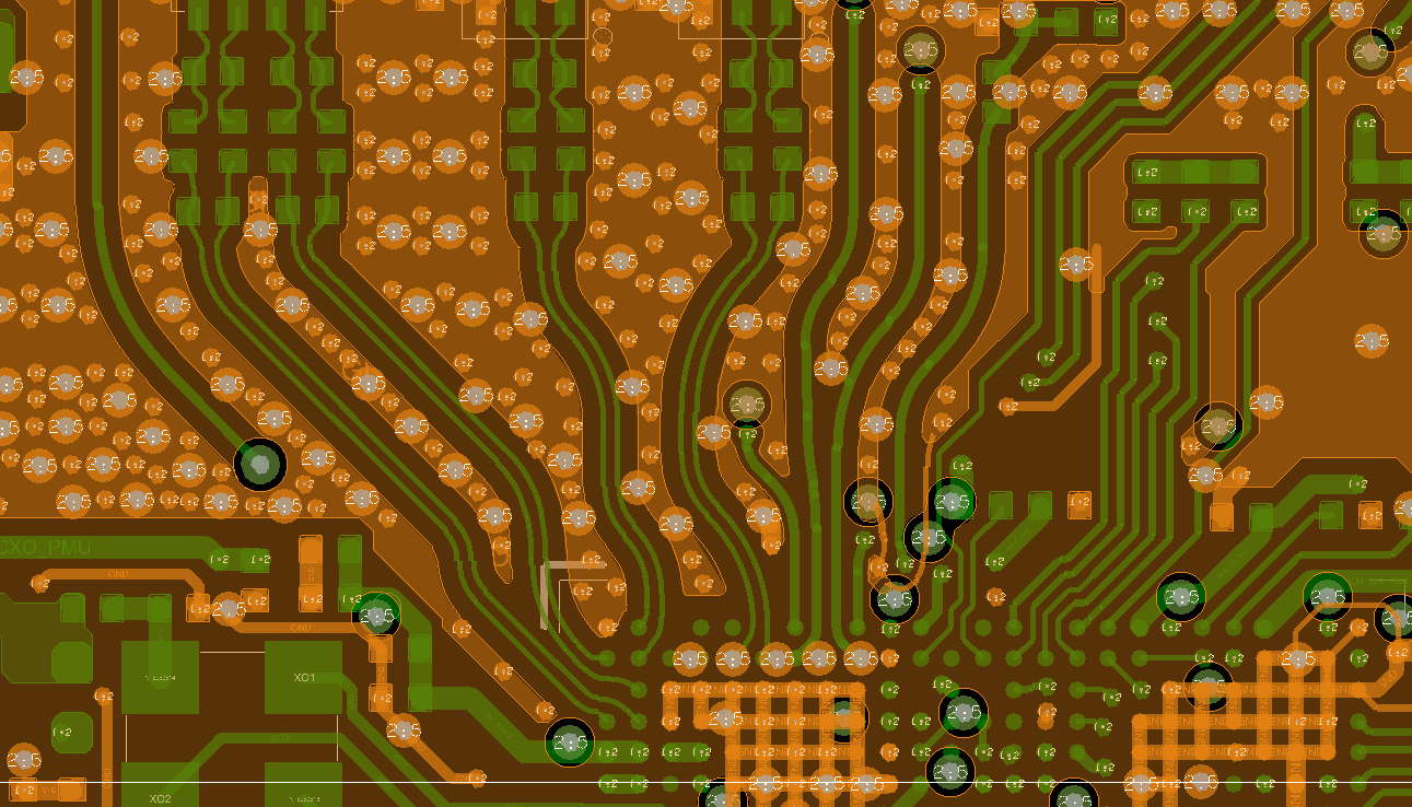
- Single-stage HDI with blind, buried and through-hole vias
- Project interfaces
- LPDDR3 · PCIe · USB 3.0 · USB 2.0 · LVDS · LAN · RF
PCB layout scope
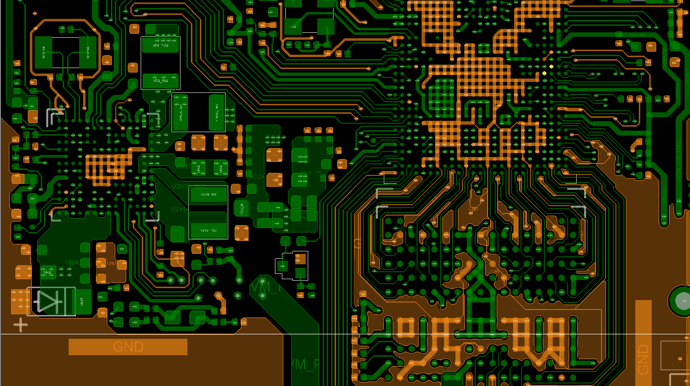
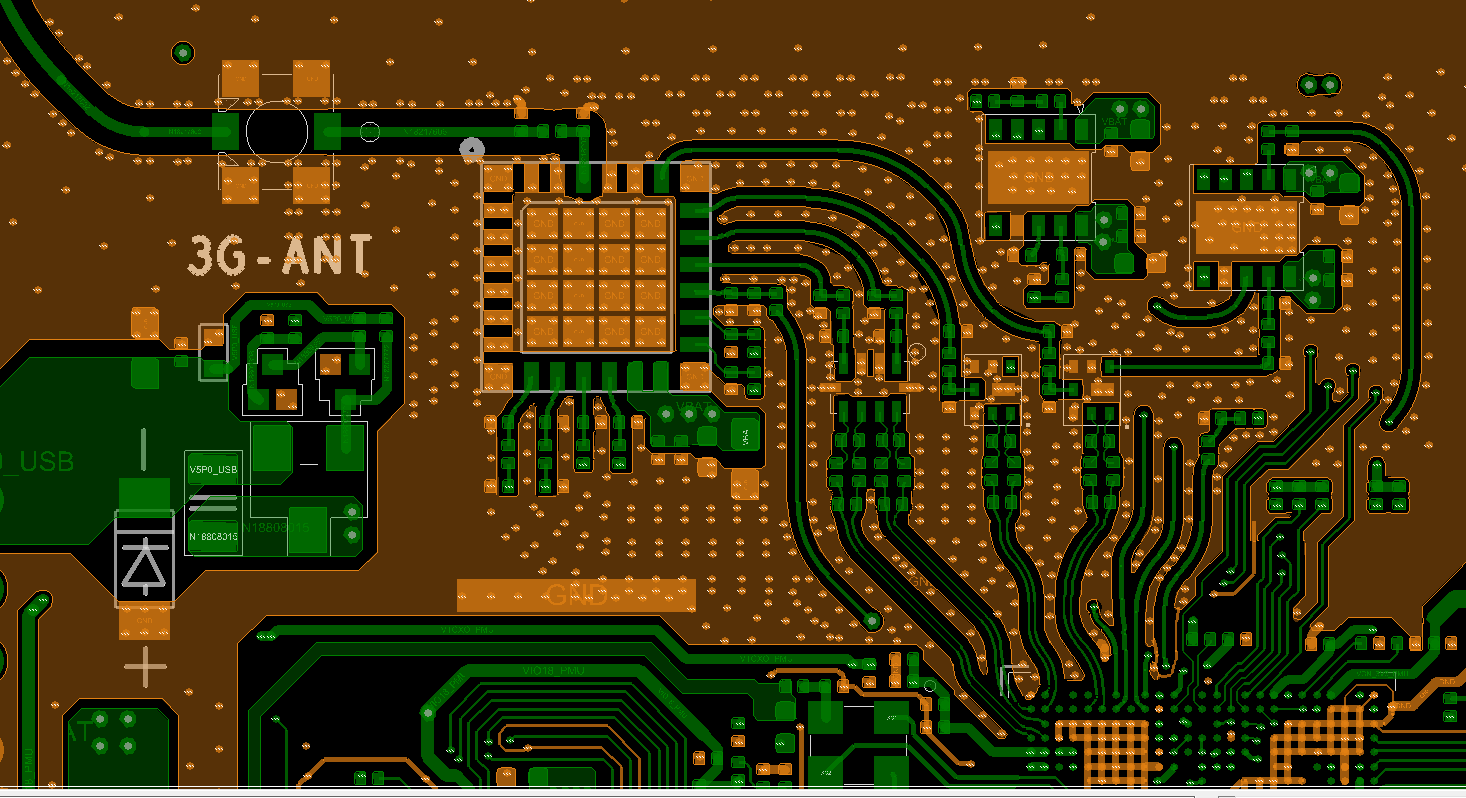
PCB placement and routing for a 3G tablet mainboard, covering processor and memory connections, power routing and the RF area within a compact board outline. The specifications above refer to the mainboard.
Project imagery
Six original CAD views show the board overview, processor routing, the 3G RF area, via detail and selected routing details. Project identifiers are redacted from the overview.
LET’S BUILD YOUR NEXT BOARD
Have a PCB project to discuss?
Send us your schematic, design requirements or existing PCB files.