
SELECTED WORK / PCB LAYOUT
HiSilicon Hi3559 SOM + Carrier Board
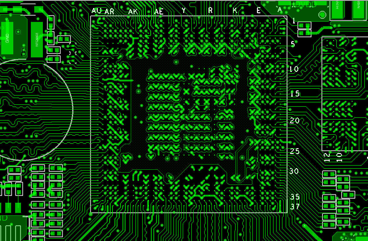
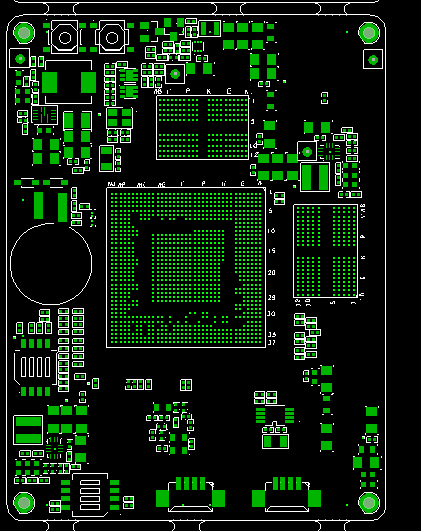
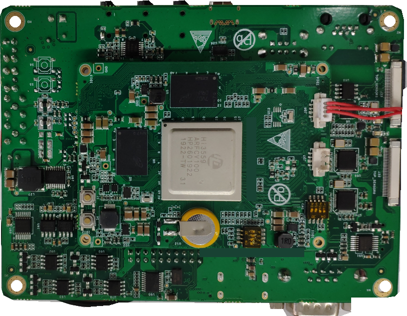
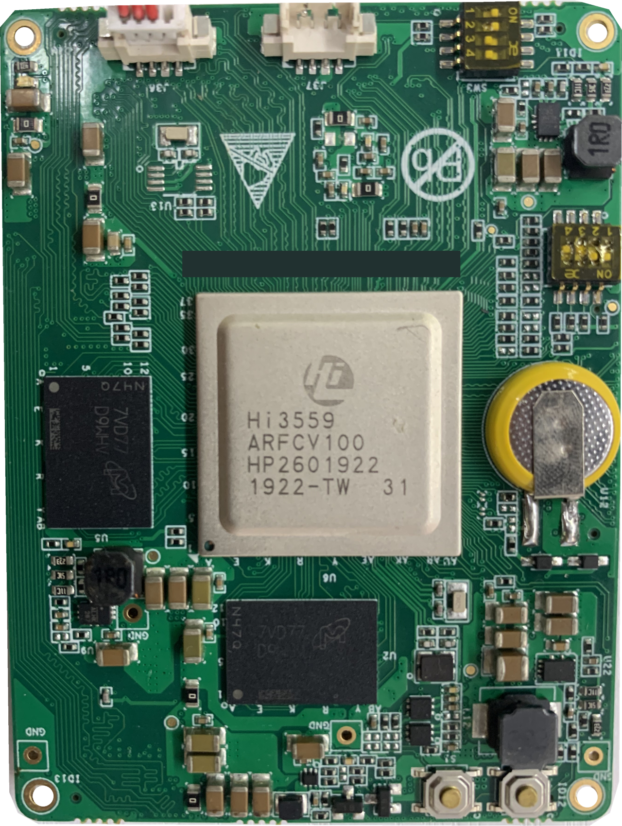
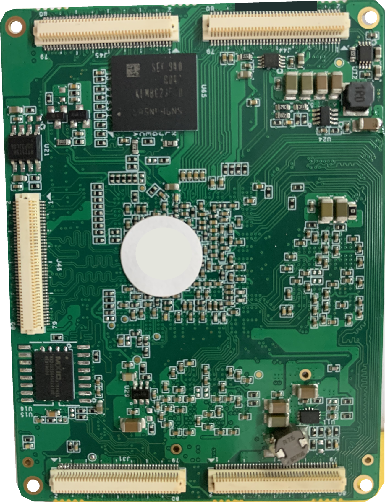
PCB layout for a HiSilicon Hi3559-based SOM and carrier-board project. The 8-layer SOM fits within a 60 × 80 mm outline, with memory and multiple peripheral interfaces integrated into the design.
Use the arrows, thumbnails or swipe to browse. Select an image to view full size.
- Platform
- HiSilicon Hi3559
- SOM layer count
- 8 layers
- SOM dimensions
- 60 × 80 mm
- Project interfaces
- USB 2.0 · USB 3.0 · PCIe 2.0 · MIPI · LPDDR4 · MDI · HDMI
PCB layout scope
SOM core-board and carrier-board PCB layout. Layer count and dimensions above refer specifically to the SOM; carrier-board specifications are not listed.
Project imagery
Original layout views show SOM component placement and routing detail. Photographs show the assembled SOM and carrier board, plus both sides of the SOM. Customer identifiers are redacted and backgrounds removed; chip markings and component references are retained.
LET’S BUILD YOUR NEXT BOARD
Have a PCB project to discuss?
Send us your schematic, design requirements or existing PCB files.