
HIGH-DENSITY PCB LAYOUT / 06
12-Layer 2-Stage HDI — LPDDR5 BGA Fanout
496-Ball BGA Escape Routing with Stacked Microvias
Project Overview
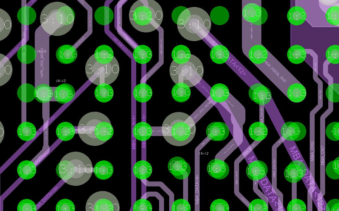
This case study presents a high-density PCB layout featuring a 496-ball BGA associated with an LPDDR5 memory interface, implemented on a 12-layer PCB using a two-stage stacked-microvia HDI architecture.
The primary engineering focus was to plan the BGA breakout, manage routing congestion, and coordinate layer transitions with the high-speed memory interface requirements.
Key Design Parameters
- PCB Stackup
- 12 Layers
- HDI Architecture
- 2-Stage
- Microvia Structure
- Stacked Microvias
- BGA Package
- 496 Balls
- Memory Interface
- LPDDR5
- Engineering Focus
- BGA Escape, HDI Via Planning, High-Density Memory Routing
Engineering Challenges
Dense BGA Escape Routing
The 496-ball package presented limited routing channels, particularly for signals located within the inner ball rows. Routing access had to be considered together with via placement and available signal layers.
Two-Stage Stacked Microvia Planning
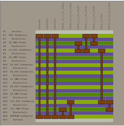
The stacked-microvia architecture provided additional interlayer routing flexibility. Microvia placement required coordination with pad geometry, fabrication rules, and the intended layer-transition strategy.
LPDDR5 Routing Constraints
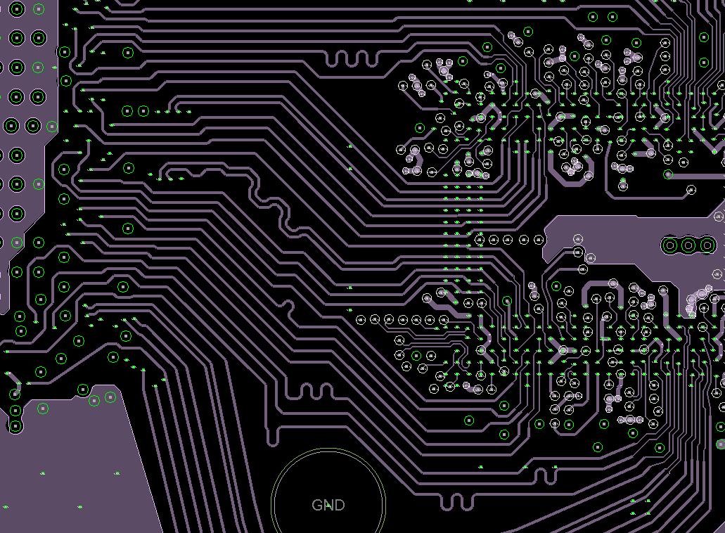
The routing strategy considered signal grouping, DQ/DQS relationships, clock and command/address routing, timing constraints, and reference-plane continuity.
Manufacturing Feasibility
Stacked microvias introduce additional fabrication considerations, including via filling, plating, registration, and reliability. The layout strategy therefore needed to account for the PCB fabricator’s HDI capabilities.
Stackup and Via Planning
Engineering Approach
1. Plan Escape Paths Across the 496-Ball BGA
For this 496-ball BGA, breakout planning connected access from the inner ball rows with the routing space available outside the package. Fanout paths, via placement and signal-layer allocation were considered together to avoid moving congestion from the BGA region into the memory-routing area.
2. Coordinate the Two-Stage Stacked-Microvia Transitions
The confirmed two-stage stacked-microvia architecture formed the basis for planning transitions in the dense BGA region. Transition choices needed to remain consistent with the approved stackup and the fabricator’s construction rules, including stacked-via filling and registration requirements. The supplied stackup view provides context; it does not establish an assumed L1–L2–L3 construction.
3. Carry LPDDR5 Constraints Through the Breakout
LPDDR5 routing decisions linked the BGA escape paths to memory-interface signal grouping, DQ/DQS relationships, and clock and command/address routing. Layer transitions and local routing adjustments had to be considered alongside timing requirements and reference-plane continuity, rather than treating fanout and memory routing as separate tasks.
4. Keep Layout Choices Aligned with HDI Fabrication
For this 12-layer HDI layout, via placement and routing choices needed to fit the board manufacturer’s approved process. Stacked-microvia construction, via filling, plating and registration are fabrication review points; the images do not by themselves establish process qualification or reliability results.
Engineering Takeaway
This project illustrates how stacked-microvia planning, BGA breakout strategy, and memory-interface routing constraints must be considered together in a high-density multilayer PCB design.
HDI / MEMORY INTERFACE LAYOUT
Need Support with a Complex HDI Layout?
CHIWIN provides PCB layout support for high-density BGA breakout, multilayer HDI routing, and high-speed memory interfaces.